Professor Kim Sae-hyeon Advances Commercialization of 'Bending Display' N
No.88854- Writer pr
- Date : 2016.04.06 09:57
- Views : 7527
Joint research with POSTECH, developed high performance/nano-patterning organic semiconductor process technology
Expected to use in next-generation flexible display, memories, and other electronic materials
Poster paper in recent academic journal in top 1.5% materials science sector
[March 23, 2016]
A local joint college research team developed a technology that can advance the commercialization of next-generation flexible displays.
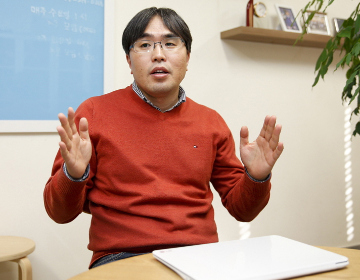
YU School of Chemical Engineering Professor Kim Sae-hyeon (37) and his research team worked together with the research team of Park Chan-eon of Pohang University of Science and Technology and successfully developed the 'High Performance Nano-Patterning (process of configuring an image on a thin film) Organic Semiconductors (organic compound with semiconductor characteristics) Process Technology'. This technology concentrated high performance organic semiconductors into nano (10-9) meter intervals.
Unlike inorganic semiconductors such as silicon, organic semiconductors are light and flexible so they can be applied to various electronic materials. Furthermore, it is relatively inexpensive so it can be mass produced and has been receiving a lot of attention for the development of next-generation electronic materials. However, it faces difficulties in commercialization due to its lower performance and limitations in integration technologies. Thus, the research team conducted studies focusing on the need to configure high performance organic semiconductor crystals and for the process development that can pattern it in nano-units.
The research team explained, "We conducted research on a process method from the idea of the 'capillary phenomenon' where liquid follows the tube and rises when there is a narrow and long tube. We produce a mould with nano-meter patterns to make it in the form of a capillary and use it as the frame for filling it up with semiconductor solutions." They added, "We found that the organic semiconductor solution between the moulds at the lower vexil and nano-structure patterns rose in the nano-sized capillary tubes and naturally generated nano-sized single crystals (solid that is regularly generated according to a constant crystall axis for the entire crystals). In result, we were able to produce large-area organic semiconductors aligned in 50 nanometer intervals for 50 nanometer organic semiconductor single crystals'.

Professor Kim said, "The research outcome is very significant in that it unified the high performance organic semiconductor generation and fine patterning work, which are important issues in commercializing organic semiconductors," and added, "As technologies for commercializing organic semiconductors developed, it is expected that it can be used in a broad range of next-generation electronic elements such as flexible displays, electronic paper, wearable sensors, memories and batteries.
Meanwhile, this study was carried out as part of the senior researcher support project and new research support project overseen by the Ministry of Science, ICT and Future Planning and the National Research Foundation. The research results were published as the poster paper of the latest issue (February 24) of the globally acclaimed academic journal, <Advanced Materials (impact factor, IF, 17.493)>, which is in the top 1.5% of the materials science sector.